Readings (from BOH3)
Chapter 3:Section 3.1
Section 3.2
Section 3.3
Section 3.4
Section 3.5
Buffer Overflow
Copying %rax to %rip:
jmp %rax
Copying %rip to %rax:
call get_rip
get_rip:
pop %rax
or
lea (%rip), %rax
BOH3 Section 3.10.3
An Introduction to Computer Networks: An
Actual Stack-Overflow Example
SRAM: 6 transistors
DRAM: 1 capacitor, maybe a transistor or diode. Needs refresh ~30x/sec
n-bit ram: classic n/2 x n/2 layout, two n/2-decoders.
(this is no longer completely accurate; BOH3 has a better description. The above is sort of a 2nx1 DRAM. What really happens is that the entire row is extracted first, all in parallel, and then the desired column of that row)
Fast-page-mode DRAM: that extracted row is used for as many columns as necessary.
Double-data-rate Synchronous DRAM: both clock up and clock down can be used for reads. DDR: 2 bits at a time, DDR2: 4 bits, DDR3: 8 bits
Memory Address Bus / Memory Data Bus
Northbridge
Random memory access times are ~100 clocks. Memory is slow.
Disks: 5 ms seek / 5 ms rotational latency ?
SSD: changes a lot
CPU view of disk: a big array of logical blocks
DMA
elevator algorithm
SSDs
"SSDs have completely replaced rotating disks in portable music devices" The original iPod actually did have a spinning-rust disk.
There are still HUGE amounts of data kept on spinning-rust.
Spatial locality: stride-1, stride-k
Instruction locality: avoid code with lots of jumping (though branch-predictable jumps are ok)
Cache replacement
Which line do we overwrite? cache placement: where can we put the replacement line? These are the same question, but they are different issues.
L1i, L1d
L2
L3
S sets of E lines each; each line contains a block of B bits. In many cases, E=1. Blocks typically contain 64 bytes, and always hold memory aligned on a 64-byte boundary.
Each block needs a valid bit, and also a set of tag bits to indicate what memory address range is stored in that block.
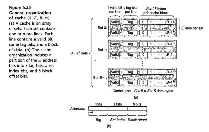
E=1: direct-mapped cache. A set is a block, plus valid bit and tags.
Suppose we are going from 4GB DRAM (32 bits) to 4 MB direct-mapped cache (22 bits), with 64-byte lines (6 bits). There are thus 216 cache sets of 26 bytes each.
For a given memory address, the low-order 6 bits (bits 0-5) identifies the byte within a line. The next 16 bits, bits 6 through 21, identifies the cache line; these are sometimes called the cache-index bits. The remaining 10 bits, 22-31, represent the tag. The 64-byte-aligned memory address m (that is, last 6 bits zero) will always map to the same line as m+222.
Conflict misses (BOH3 p 622)Note that bits 6-21 of any memory address determines its cache line. There are no alternative placements. This means that if we load something else with the same 6-21 bits, the cached value is lost. Here is an example: .
float
dotproduct(float x[N], float y[N]) {
float sum = 0.0;
for (int i=0; i<N; i++) {
sum += x[i]*y[i];
}
return sum;
}
We will assume 64-byte cache blocks, and two cache sets (lines). What we hope is that, as we go through 16 floats, all the x[i]'s and all the y[i]'s should be in the cache, the x[i]'s in one line and the y[i]'s in the other.
However, suppose that x is aligned on address 0x40000, and y starts at address x+222 = 0x80000. Then, for any given i, &x[i] and &y[i] will have addresses differing by 222, and so will map to the same cache block. They cannot share. For every i, there will be two cache misses, one for x[i] and one for y[i].
BOH3 has a smaller-scale example of this.Would using the high-order 16 bits (16-31) as the cache-index bits help any? No. Then, if we were traversing just one of the arrays, the &s[i] addresses would have the same cache-index bits for 210 blocks in a row, so we would have multiple cache misses.
Here, one block of memory can be stored in any of several lines. In the extreme case, one block of memory can be stored anywhere. In the more moderately priced category, each set might have 16 lines (versus 1), and a value can be stored anywhere. To match the right tags in a given set, usually associative memory is used.
In the ultimate case, with a fully associative cache, we take bits 6-32 and find the block that has these bits in its tag. We then fetch the corresponding data. Associative memory, sometimes called content addressable memory or CAM, looks something like this:

This picture shows the input tags, at the left, being converted to a normal cache memory address. It is also possible for the output to be the matching contents corresponding to the input tag.
With associative caches, we need a replacement policy. One classic approach is least-recently used, or LRU. The problem with LRU is that we need to keep track of the times of each access; usually this is prohibitive. A reasonable alternative is random replacement, or even round-robin replacement.
When there are multiple layers of caches, eg L1, L2, L3, if we write to L1, what do we do to L2 and L3? If we write to those also, this is called write-through. If we leave those alone until that cache line is updated by something else, that is write-back. Getting write-back to work well is difficult, though, when it does, the write-backs can often be done when the memory bus is otherwise idle.